Research
Semiconductor Materials → Flip-Chip Packaging → Optical Design → AIoT Systems → Electronic Metrology
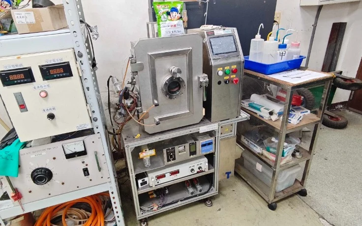
💡 High-Power LED Flip-Chip Packaging & Micro-Bonding
Focusing on high-power and automotive optoelectronics: developing lead-free transient liquid phase (TLP) bonding, Au-Sn eutectic submounts, and anti-settling phosphor encapsulation for high thermal fatigue resistance and chromatic uniformity.
Key Technologies
- Lead-free transient liquid phase (TLP) bonding: Al-Ge-Sn and In alloys to resolve thermal fatigue and voiding in high-power chip joints
- Flip-chip bonding on submounts: zincate-processed Al-based Au-Sn eutectic micro-joints with SiC and AlN stress buffer layers
- High-thermal-dissipation carriers: patterned silicon submounts and planar glass flip-chip substrate micro-electrode routing
- White LED phosphor encapsulation: anti-settling dispensing, continuous electrophoretic deposition (EPD), and precision molding to eliminate yellow-ring artifacts for uniform emission
🎓 Representative Theses by Lab Alumni
- 📜 Structural analysis of AlGeInSn bonded joints prepared by transient liquid phase bonding
- 📜 The Study of The Low Temperature Flip-Chip Package by Applying AlGeSn-Based Transient Liquid Phase Bonding Technique
- 📜 AuSn Eutectic Stack Layer on Al substrate Used Zincating and Discussion of Flip-Chip package
- 📜 Application of Al-Ge-Cu-Zn-Sn Flip-Chip Substrate for Glass
- 📜 Anti Precipitation Technique of Phosphor Pasting for Promotion of Yield
- 📜 Development of high power white LEDs by adopting the continuously electrophoretic process technique
- 📜 Improvement of the packaging process and technique for the LED mass production
- 📜 The development of the flip chip patterned silicon and the integrated silicon-aluminium submounts for high power LEDs
Applications
🤖 Smart AIoT & Industrial Sensing Systems
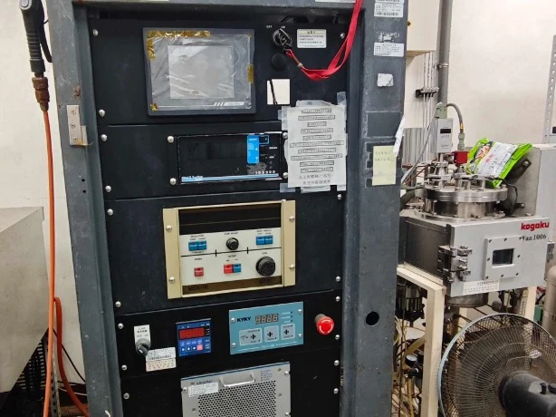
Integrating embedded microcontrollers, edge vision, and IoT cloud platforms: developing real-time metalworking fluid quality monitoring, smart utility metering, self-powered rehabilitation aids, and telemetry.
Key Technologies
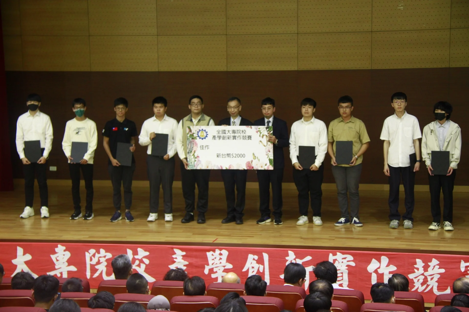
- Falling-ball cutting fluid sensor: integrating MCUs and automated fixtures for precise viscosity and oil concentration telemetry (2023 National Competition Award)
- Edge AI vision & optical inspection: MCUs with YOLO object detection and optical transmittance to monitor fluid contamination and emulsification in real time
- Edge meter reading & IoT telemetry: Raspberry Pi, OpenCV, OCR, and IoT cloud for automated real-time digitization of analog utility meters
- Kinetic harvesting & smart healthcare aids: pedal power generation integrated with senior rehabilitation telemetry (2024 Innovation Award) and mobile-controlled wheelchairs
🎓 Representative Theses by Lab Alumni
- 📜 Applying Pedal Power Generation in Smart Elderly Health Rehabilitation System
- 📜 Metalworking Fluids Oil Concentration Measurement: A Sensor System Utilizing the Falling Ball Method
- 📜 Traditional Water Meter Numerical Automatic Reading System Based on Raspberry Pi: Integration of OpenCV, OCR, and IoT
- 📜 The concentration measurement system for metal working fluid based on microcontroller and YOLO object detection
- 📜 Design of an Intelligent Vacuum Cleaner System Based on Image Recognition Technology
- 📜 The Study of Optical Sensor for Sensing the Quality of Cutting Fluids
- 📜 Mobile phone remote control electric wheelchair with cloud function
- 📜 An IOT-based water level monitoring device with warning system
Applications
🔬 Semiconductor Thin-Film Metrology & VOx Interface Physics
Leveraging our core metrology strengths: non-contact optical thin-film thickness prediction models, micro-probe contact resistance analysis, and connected temperature-dependent (I-V-T) test benches.
Key Technologies
- Non-contact optical film metrology: custom automated fixture predicting nanometer thickness from reflection CIE Lab chromaticity and phase shifts of Ge ultra-thin films
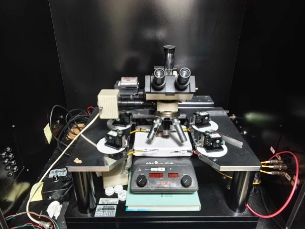
- Contact resistance metrology: extracting specific contact resistance and annealing characteristics of composite metal/VOx interfaces via CTLM and micro-probe stations
- Custom connected temperature-dependent I-V analyzer: integrating microcontrollers and automated DAQ to scan carrier transport and TCR under controlled thermal environments
- Physical electronics & micro-sensors: custom test bench for thin-film thermal diffusivity and interdigital transducer (IDT) sensors for liquid electrical conductivity
🎓 Representative Theses by Lab Alumni
- 📜 Portable low-cost networked semiconductor temperature-dependent electrical property analysis system
- 📜 Design a Measurement System for Measure Thermal Diffusivity of Thin Films
- 📜 The IDT sensing system applied to measure the conductivity of diluted acid solution
- 📜 Characterization of the Contact of Vanadium and Vanadium Oxide by Low Temperature Annealing Process
- 📜 Design an Automatic Fixture System for Establishing the Relationship between the Thickness and Chromaticity of Ultra-thin Film
- 📜 Predicting the Thickness of Ultra-thin Films by the Chromaticity and Phase of the Germanium Ultra-thin Film
- 📜 Study on the Specific Contact Resistivity of the Composite Metal-VOx Interface Evaluated by Using CTLM method
- 📜 Study on Chromaticity Related to Thickness of Germanium Ultra-thin Film
Applications
❄️ Advanced Thermal Management & Microchannel Cooling
Addressing thermal bottlenecks in power optoelectronics and microprocessors: developing microchannel coolers, bonded copper fluid channels, TEC active thermoelectric cooling, and high-thermal-conductivity films.
Key Technologies
- Active microchannel coolers: designing fluidic microchannel architectures for conjugate thermal dissipation in high-power LED modules
- Copper microchannels with low interface resistance: Al-Ge thin films for copper bonding to reduce interface thermal contact resistance
- Junction temperature (Tj) prediction & TEC control: precise thermal models under varying drive currents, paired with TEC thermoelectric closed-loop cooling
- High-thermal-conductivity film dissipation: AlN thin-film deposition and electro-thermal separation for LED projection lamps and bulbs
🎓 Representative Theses by Lab Alumni
- 📜 Prediction of Junction Temperature for LED Operated at Various Current for Mass-production.
- 📜 Study on the Properties of Microchannels with Copper Bonded by Al-Ge Thin Films
- 📜 Applying microchannel cooler to study the heat dissipation of the LED module
- 📜 Research of TE Cooler Commercialization
- 📜 Plastic LED bulb with active heat spreading
- 📜 Development of the LED Injecting Modules Based on the Thermal-Electric Separation
- 📜 Study of AlN Thin Films for High-Power Light Emitting diode by High Heat Conduction Layer
- 📜 Study of heat transfer effect of high power LEDs by high heat conduction layer
Applications
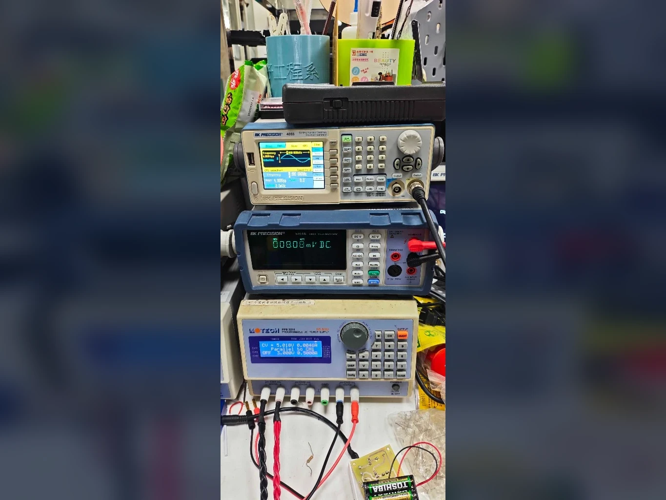
🌈 Optical Design, Backlight Modules & Display Technologies
Advanced optical simulation and microstructures: optical optimization for Mini LED backlights, quantum dot wide color gamut, thin light guide plate (LGP) dot patterns, and secondary optics lenses.
Key Technologies
- Mini LED & QD backlights: optical lens optimization for Mini LED modules, integrating quantum dot films for wide color gamut and high luminance uniformity
- Thin light guide plates & micro-dots: optimizing micro-dot optical patterns for ultra-thin LGPs and light-guide-free edge-lit backlight architectures
- Energy-saving secondary optics: luminous intensity distribution design for direct-lit secondary lenses, applied to uniform LCD backlights and streetlights
- Color mixing prediction & light extraction: CIE chromaticity coordinates and luminance modeling for RGB mixing, and patterned ITO to enhance chip light extraction
🎓 Representative Theses by Lab Alumni
- 📜 Optical optimization of Mini LED backlight module
- 📜 Optimize the color gamut of the quantum dots backlight module
- 📜 Optoelectronic Effect of the reflection Wall Process
- 📜 Prediction of Cie Coordinates And Luminosity for The Mixed Light of Three Primary Colors
- 📜 Analysis of Light Extraction Characteristics for LED Chips With Patterned ITO
- 📜 Design of the Energy-saving Direct-type second LENS LED Backlight Module
- 📜 The Application of MMA/SM Copolymers for Back Light Module Light Guide Plate
- 📜 Optimum Optical Design of Thinned Light-guide Plate Pattern
Applications
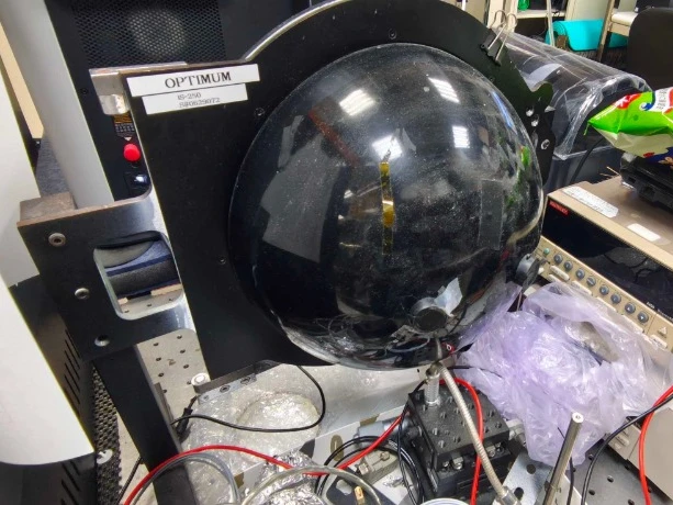
☀️ Photovoltaics, Wide-Bandgap Semiconductors & Green Tech
Expanding green optoelectronics and sustainable tech: research on CdS thin-film photovoltaics, CPV systems, AlGaN/GaN wide-bandgap power devices, and semiconductor exhaust gas abatement.
Key Technologies
- Thin-film photovoltaics: chemical bath deposition of cadmium sulfide (CdS) thin films, optimizing photoelectric conversion efficiency and heterojunctions
- Concentrated photovoltaics (CPV) & anti-reflective coatings: optical efficiency analysis of CPV systems, developing multilayer anti-reflective coatings to reduce reflection loss
- GaN wide-bandgap power devices: physical characterization of AlGaN/GaN 2D heterostructures and fabrication of high electron mobility transistors (HEMTs)
- Semiconductor gas abatement & dust removal: UV/thermal cracking optimization for nitrous oxide (N2O) process gas and micro-mist abatement for SiO2 dust
🎓 Representative Theses by Lab Alumni
- 📜 The study of cadmium sulfide thin films applied on solar cells
- 📜 The efficiency analysis and study of the collective photovoltaic collector system
- 📜 Study of the Encapsulation Efficiency for Light-Emitting Diode and Solar Cell by Applying the Optical Antireflection Films
- 📜 The Study of AlGaN/GaN Two-Dimensional Heterojunction Structures
- 📜 Fabrication and study of algan/gan high electron mobility transistor
- 📜 Characterization of ingan-based photodetectors
- 📜 Optimizing the Decomposing Efficiency of the Nitrous Oxide Gas Generated in the Semiconductor Process
- 📜 Discussion on Treatment of SiO2 Dust by Micro Mist Dust Removal System
Applications